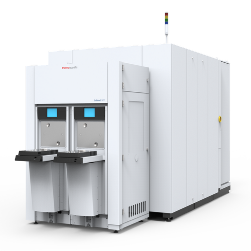

TEM analysis sample preparation workflow for automated, high throughput semiconductor wafer analysis.
The Thermo Scientific ExSolve wafer TEM prep (WTP) DualBeam (FIB-SEM) dramatically reduces the cost and increases the speed of sample preparation, providing semiconductor and data storage manufacturers with quick and easy access to the data they need to verify and monitor process performance. The ExSolve DualBeam can prepare site-specific TEM lamella, sampling many sites per wafer in a fully-automated process inside the fab, giving semiconductor manufacturers much more information than conventional approaches, while at the same time reducing the capital cost of sample preparation by up to 70 percent.
The ExSolve WTP DualBeam system is an automated, high-throughput sample preparation system that can prepare site-specific, 20 nm thick lamellae on whole wafers up to 300 mm in diameter. It is part of a fast, complete workflow that includes Thermo Scientific TEMLink, and the Thermo Scientific Metrios TEM. The ExSolve DualBeam includes FOUP handling and is designed to be located in the fab near the manufacturing line.
The ExSolve WTP DualBeam workflow addresses the needs of customers that require automated, high-throughput sampling at advanced technology nodes. It complements the capabilities of the Thermo Scientific Helios NanoLab DualBeam 1200AT, which provides more flexible, operator-directed, sample preparation methods, along with additional capabilities such as high-resolution scanning electron microscopy (SEM) imaging and analysis.
