
FIB-SEM TEM sample preparation for the semiconductor industry, enabling full-wafer analysis.
Demand for high-performance, energy-efficient electronics is driving the development of advanced devices with ever smaller, more densely packed features and complex 3D structures. Ramping production of these cutting-edge microprocessors, memory devices, and other products is extremely challenging and requires high-resolution, atomic-scale analysis of features buried deep within the device. Transmission electron microscopy (TEM) is increasingly becoming the go-to technique for this kind of analysis and relies on high-quality samples produced with focused ion beam (FIB) milling.
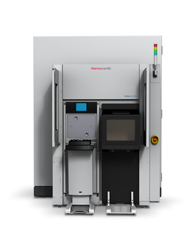
The Thermo Scientific Helios 5 EXL DualBeamis a 300mm full-wafer focused ion beam scanning electron microscope (FIB-SEM), designed to address TEM sample preparation challenges in the semiconductor industry. The Helios 5 EXL DualBeam is capable of preparing samples for today’s most advanced process nodes, including sub-5nm and gate-all-around technology.
Maximizing sample throughput and productivity
Utilizing advanced machine learning and closed-loop end pointing, the Helios 5 EXL DualBeam delivers enhanced cut placement precision and enables you to consistently extract high-quality lamella from your most challenging samples.
Advanced machine-learning automation capabilities make ultra-thin TEM sample generation routine and consistent, providing unparalleled, sub-nanometer insight into more interfaces, films, and profiles to measure at sub-nanometer resolution. The Helios 5 EXL DualBeam ensures efficient and consistent TEM sample preparation workflows by combining wafer and defect navigation with recipe definition and execution in a single, fully integrated program. This automation supports a higher tool-to-operator ratio, maximizing sample throughput and technical resource productivity.